
Radar SoC
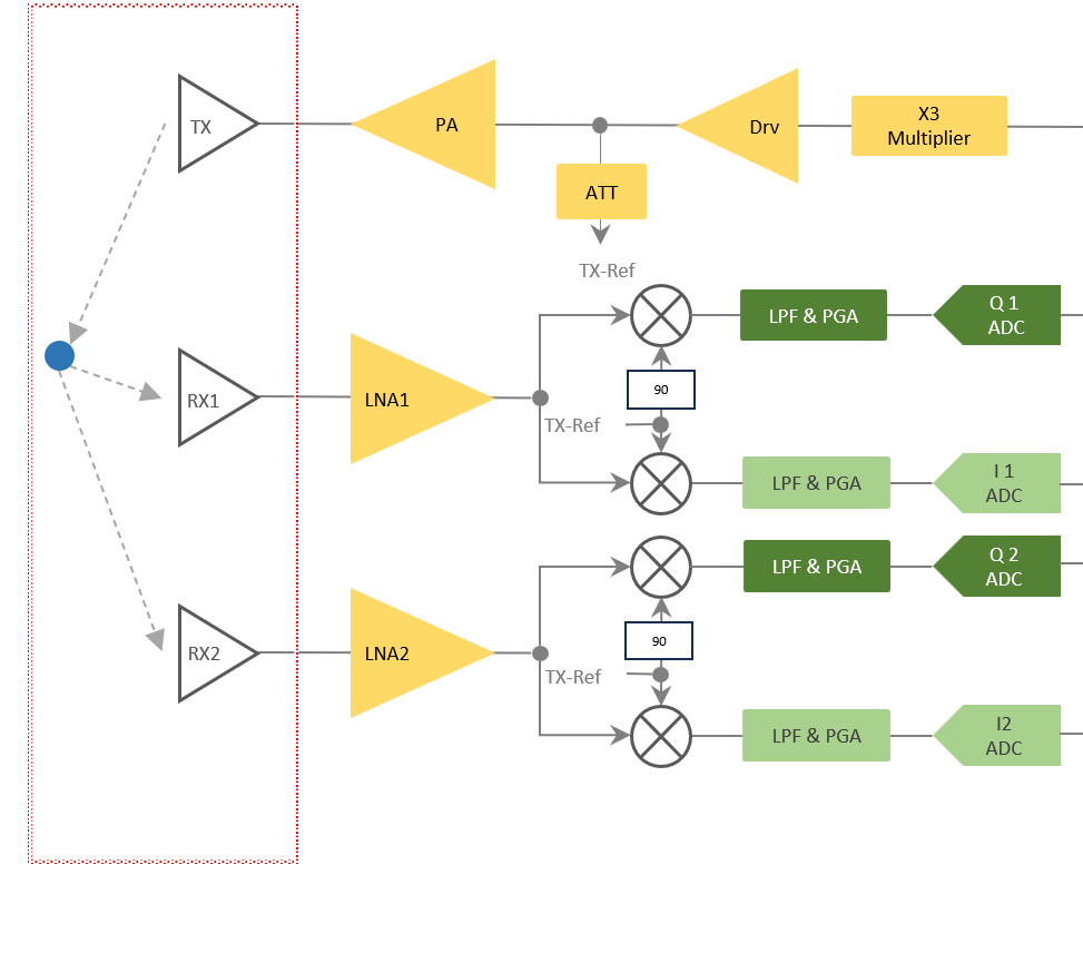
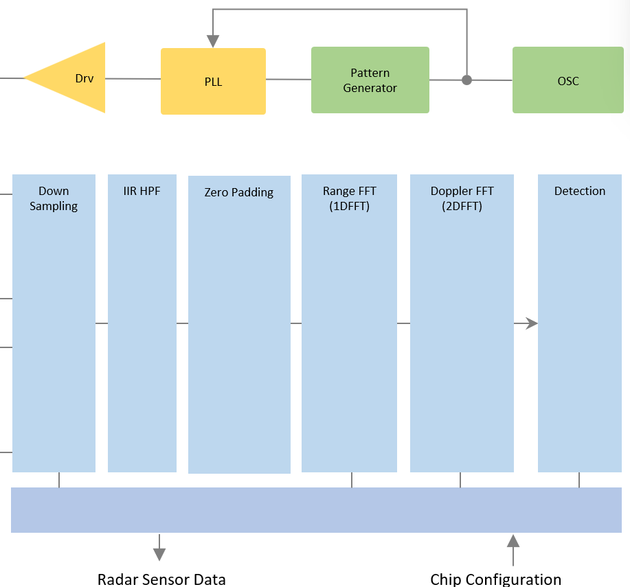
Internal blocks of general radar sensor SoC.
1. Radar System Block
2. Features
| Feature | Description | |
| Radar Type | 24 GHz K-band highly integrated FMCW radar sensor SoC | |
| Bandwidth | Up to 1 GHz bandwidth FM tuning range | |
| Integrated Blocks | Integrated signal generator, low phase noise PLL, transmitter, receiver, baseband and ADCs | |
| TX/RX Channels | One transmit channel and one receive channel | |
| Ultra Low Power | As low as 55 μA current dissipation with 0.3% duty cycle operation | |
| TX Output Power | TX maximum output power: 12 dBm | |
| RX Noise Figure | RX noise figure: 10.0 dB | |
| Phase Noise | Phase noise @ 1 MHz offset: -97 dBc/Hz | |
| ADC | Built-in 2.5 MHz conversion rate ADC with 16 bits resolution | |
| Chirp Ramp Rate | Fast FMCW chirp ramp rate: up to 20 MHz/μs | |
| Chirp Linearity | High FMCW chirp linearity of 0.45‰ at 250 MHz tuning range | |
| TX Power Control | Precise TX power control enhanced by on-chip power detector and temperature sensor | |
| Hardware Accelerator | Built-in hardware accelerator, support complex FFT and CFAR function | |
| Configuration Interface | I2C / SPI / UART | |
| Data Output Interface | DS RAW / SPI (master/slave mode) / UART | |
| Power Supply | Support flexible power supply modes | |
| Package | 4 mm × 4 mm QFN32 package | |
| Temperature Range | Junction temperature range: −40°C to 105°C |
2. PIN desription
| Pin Name | Type | Description | |
| NC | NC | No electrical connection internally. It may be left floating or connected to ground | |
| RSTN | IN | External hardware reset input. A logic LOW on this pin resets the device, causing internal digital circuit to take their default states | |
| V_R | Power | 1.6 V analog power supply for RX sections | |
| PLL_VC | IN | Connected to external loop filter to drive the internal VCO | |
| RF_RES_1 | OUT | Reserved RF pin, connect to Pin 8 | |
| V_T | Power | 1.6 V analog power supply for TX sections | |
| RF_RES_2 | IN | Reserved RF pin, connect to Pin 6 | |
| TX | OUT | Single-ended transmitter output port | |
| REXT | IN | Current bias circuit input, connect to ground with a bias resistor | |
| XOUT | OUT | Crystal oscillator Output port | |
| XIN | IN | Crystal oscillator or external clock Input port | |
| VDD_A | Power | 3.3 V power supply for analog domain | |
| DCDC_SW | OUT | DCDC regulator switch node. Connect to the power inductor | |
| VDD | Power | 3.3 V power supply for the DCDC converter and digital domain | |
| V_A | Power | 1.6 V power supply for analog circuits | |
| V_D | Power | 1.6 V power supply for digital circuits | |
| I2C_SDA | OD | Configuration_I2C_SDA: Configuration channel I2C data I/O (open drain) | |
| I2C_SDA | IN | Configuration_SPI_MOSI: Configuration channel SPI data input | |
| I2C_SDA | IN | Configuration_UART_RX: Configuration channel UART receiver | |
| I2C_SCL | IN | Configuration_I2C_SCL: Configuration channel I2C clock | |
| I2C_SCL | IN | Configuration_SPI_SCLK: Configuration channel SPI serial clock | |
| I2C_SCL | OUT | Configuration_UART_TX: Configuration channel UART transmitter | |
| C_SPI_CSN | IN | Configuration_SPI_CSN: Configuration channel SPI chip select enable | |
| C_SPI_MISO | OUT | Configuration_SPI_MISO: Configuration channel SPI data output | |
| C_SPI_MISO | IN | Chip pin mux function, see Table 5-2 | |
| FUN_SEL | IN | Chip pin mux function, see Table 5-2 | |
| UART_TXD | IN | Standby mode pin mux function (internally pull down), see Table 5-4 |

Radar Sensor SoC & Module

WiFi IoT Module

5G/LTE/CAT-M1/NB-IoT

WiSUN/HaLow/Thread Module
