Baseband and Signal Conditioning
The baseband stage includes LPF, PGA, and ADC,
where the beat signal is filtered, amplitude-adjusted, and digitized for further digital processing.
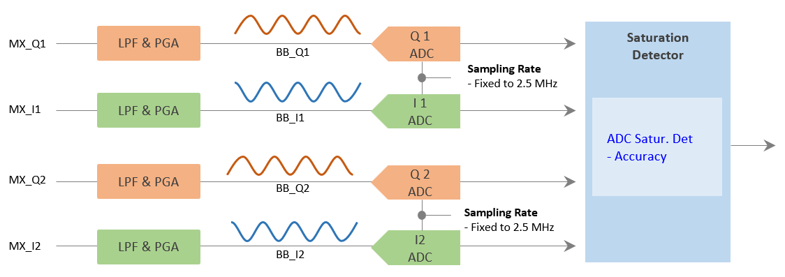
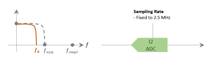
1. ADC and Nyquist Frequency
Since the ADC sampling rate is fixed at 2.5 MHz,
the beat frequency signal input to the ADC is expected to be limited to within the Nyquist frequency (1.25 MHz).
To ensure good signal quality and robust radar processing, i
t is recommended to keep the beat signal bandwidth within about 30% of the Nyquist frequency,
| Step | Technical Description | |
|---|---|---|
| 1 | The baseband bandwidth is defined by the product specifications and RF front-end signal design. | |
| 2 |
After the mixer, the baseband signal is conditioned by the LPF and PGA to limit the signal bandwidth, suppress out-of-band noise, and optimize the signal level before the ADC. |
|
| 3 | The ADC samples the conditioned baseband signal at a fixed sampling rate determined by the system (e.g., 2.5 MHz). |

1. Signal Flow and Processing
Step1. Given Condition
Allocated bandwidth: 200 MHz ← ISM Band 24.045 GHz ~ 24.245 GHz
Step2. Requirments by a customer
| Requirement | Symbol | Typical Value | Design Impact | |
| Max Range Limit | R_max | 8 m | R_max(Requirement)→B_BB(System Limit)→T_UP(Design variables) | |
| Range Resolution | ΔR | 0.75 m | Defines the RF chirp bandwidth, B_RF = c/2ΔR | |
| Max Velocity Limit | V_max | 25 m/s | Constrains the maximum allowable chirp cycle to avoid Doppler aliasing. | |
| Velocity Resolution | ΔV | 0.25 m/s | Defines the required CPI, i.e., the number of chirps per frame |
 |
 |
Step3. Chirp Design
| Name | Symbol | Typical value | Description | |
| RF Chirp Bandwidth | B_RF | 200 MHz | Selected B_RF=200 MHz within allocated band | |
| Baseband Bandwidth | B_BB | 25.4 kHz | Fixed by system bandwidth limitation (ADC/LPF). | |
| Waveform | – | CW + SAW | Continuous-wave transmission with sawtooth FMCW chirp | |
| Start Time | T_START | 20 us | typically fixed, hardware-determined settling time | |
| Down-chirp Time | T_DOWN | 150 us | typically fixed, hardware-determined reset/return time | |
| Stop Time | T_STOP | 410 us | typically fixed, hardware-determined idle/guard time | |
| Up-chirp Time | T_UP(min) | 420 us | The actual value shall be determined by considering the frame structure. |
Step4. Chirp Design Result
| Name | Formula | Example Value | Description | |
| Chirp Cycle | 1,000 us | |||
| Chirp Slope | 0.476 MHz/µs | B_RF is defined by ΔR | ||
| Baseband Signal Bandwidth | 25.4kHz |
Step5. Frame Design

2. Example Cases
32 Chirps
T_CHIRP = 1,000 us = 1ms
T_PRE=20us
T_NOP=76uS
T_2PD=22uS
T_PD = T_NOP – 2 x T_2PD = 76 – 2*22 = 32us
Frame Cycle = T_PRE + N x T_CHIRP + T_NOP = 20 us + 32 x 1 ms + 76 us = 32.096 ms
Duty Ratio = [ T_FRAME / (T_FRAME+T_NOP) ] * 100 = [ 32.096 / (0.076+32.096) ] * 100 = 99.76 %
![]()
Radar Sensor SoC & Module
![]()
WiFi IoT Module
![]()
5G/LTE/CAT-M1/NB-IoT
![]()
WiSUN/HaLow/Thread Module
![]()